
Views: 136
The new ECG MLE ™ technology offers unsurpassed flexibility, scalability and cost advantages over today’s lithography processes for high volume production
Source EV Group, a leading developer and manufacturer of equipment for wafer bonding and lithography applications in the semiconductor, microsystems and nanotechnology industries, today announced MLE ™ (Maskless Exposure), a revolutionary next-generation Lithography without mask technology designed for future End-lithography requirements have been developed for advanced packaging, MEMS, biotechnology, medical, and high-density PCB applications.
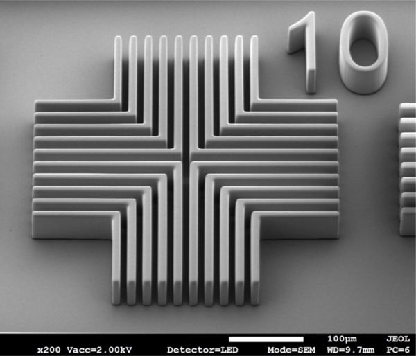
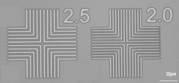
As the world’s first highly scalable maskless lithography technology for high volume production, MLE combines high resolution structuring with fast throughput and high production yield. At the same time, the considerable overhead costs usually associated with photomasks are eliminated, such as the infrastructure needed to manage and maintain the masks. In addition, MLE offers unmatched flexibility, enabling extremely short development cycles for new devices or products.
MLE Lithography without mask technology, is suitable for all wafer sizes through to panels and supports all commercially available resists thanks to a highly integrated, clustered write-head configuration and powerful UV source that supports different wavelengths.
The throughput of MLE is independent of the complexity and resolution of the substrate or chip layout and the technology achieves the same patterning performance with any photoresist materials. MLE complements EVG’s existing lithography systems, targeting new and forward-looking applications where other approaches to scalability, cost-of-ownership (CoO) and other limitations are reaching their limits.
The MLE Lithography without mask technology is already ready for demonstration in the clean rooms at the headquarters of EVG. MLE will be integrated into a new EVG product line, which is currently under development and will be announced in the next step.
“Our MLE technology excels in back-end lithography applications where other patterning technologies, such as, e.g. Stepper must compromise between performance and cost. Customers will no longer have to balance the resolution, speed, flexibility or cost of ownership of their back-end structuring applications, “said Paul Lindner, Executive Technology Director, EV Group. “During the first stages of development with a select clientele, it became apparent that a wide variety of applications could benefit from MLE, and we assume that many new areas of application will be added. As we continue to develop the first products based on this unique exposure technology, we look forward to working with additional industry partners to identify new devices and applications that will benefit from MLE. ”
New challenges for back-end lithography
As heterogeneous integration becomes the driving force behind many semiconductor developments and innovations, impacting markets such as Advanced Packaging, MEMS, and PCBs, the demands on back-end lithography are also increasing. In the field of Advanced Packaging, the required minimum resolution for Redistribution Layer (RDL) and Interposer with their steadily decreasing line / space structure sizes becomes more and more stringent.
In some cases, as much as two microns or less are targeted, while deviations in the placement of the die and the use of cost-effective organic substrates also require greater patterning flexibility. The demand for higher adjustment accuracy (overlay) as well as a high depth of field in the structuring of vertical side walls also increases. New challenges, such as Minimizing pattern distortion, as well as individual die shifting due to wafer distortion in Fan-Out Wafer Level Packaging (FoWLP) applications, and support for thick and thin resists are just a few of the criteria of today’s and tomorrow’s lithography systems for Advanced Packaging.
In MEMS production, with its complex product mix, overheads for masks and reticles have an increasing impact on total cost (CoO), while a very good focussing on trench structuring is critical. In the market for printed circuit boards and in the biotechnology and medical technology sector, the demand for greater flexibility in the structures is increasing to enable a wide range of feature and substrate sizes.
Leave a Reply